| Email:Mannan.Ali@physics.org | Chapter 6: Magneto Impedance investigation |
|---|---|
| Web: http://members.xoom.com/MannansZone/thesis.html |
6.0 Magneto Impedance investigation
6.1 Introduction
In recent years there has been a considerable upsurge of interest in the Magneto Impedance (MI) effect, found in soft, amorphous, ferromagnetic materials. The MI effect consists of large changes in the high frequency impedance Z, found in nearly zero magnetostrictive Fe/Co based alloys in the form of melt-spun wires and ribbons. The majority of the research performed has been focused on soft amorphous cobalt based alloys, in the form of wires and ribbons, even though the effect can be observed in a wide variety of materials, as the MI effect has been found to have the largest values in these materials. The intensive research into the MI effect is a result of its technological importance in the field of sensor applications [Vazquez et al (1996)]. A number of authors have shown the effect to have great potential for magnetic sensor applications [Panina et al (1994), Mohri et al (1995), Atkinson et al (1998)]. MI effects have been found to be more field sensitive than the well established giant magneto-resistance (GMR) effects found in GMR materials. These latter materials generally require large fields to obtain a GMR response of a few percent, whereas the MI materials can produce responses of a few hundreds of a percent in very small fields of the order likely to be encountered in practice. It has also been reported [Sinnecker et al (1998)] that under certain conditions the MI effect does not exhibit hysteresis effects, as is the case with GMR materials; hysteresis is undesirable for sensor applications.
The drive for magnetic sensors to become miniaturised has now increased with fresh technological demands. In these systems, sensors are now being incorporated onto commercially important substrate materials such as silicon and gallium arsenide. The advantage of this arrangement is that the sensor, and its electrical detection/analysing circuitry, can be fabricated on the same substrate. In order to make such sensor devices, it is necessary to deposit the magnetic material in the form of a thin film. It would be difficult to incorporate existing favourable MI materials into such devices in their current form of ribbons or wires. Here a different approach to the MI effect is undertaken. Magnetic amorphous films and multi-layered films produced by sputter deposition have been investigated for their potential use as MI materials in sensors. There has been only limited research done on the MI effect in thin films in comparison to their bulk counterparts [Morikawa et al (1995), Panina et al (1995)]. Mokirawa and co-workers have shown, by using multi-layered films, that it is possible to increase the MI effect in thin films compared to single layered films, thereby increasing their usefulness as sensor materials. The objective of this preliminary study into the MI effect, is to ascertain the potential use of FeSiBC films for MI sensors, and to correlate the magnetic properties with the impedance responses.
Part of this work was supported by the British Council and the Spanish Ministerio de Education y Ciencia under the Acciones Integradas program (HB95-0013).
| Growth and study of magnetostrictive FeSiBC thin films, for device applications, Mannan Ali (1999) | 130 | |
|---|---|---|
| (Online Copy) |
| Email:Mannan.Ali@physics.org | Chapter 6: Magneto Impedance investigation |
|---|---|
| Web: http://members.xoom.com/MannansZone/thesis.html |
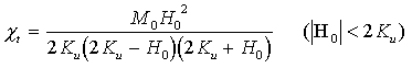
6.2 Magneto Impedance
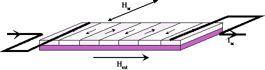
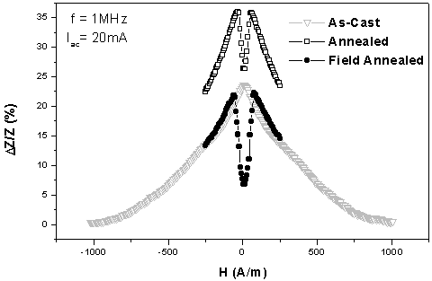
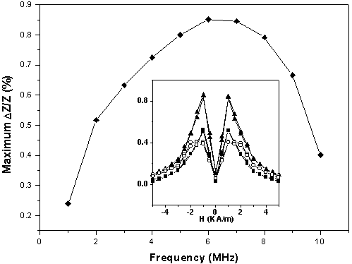
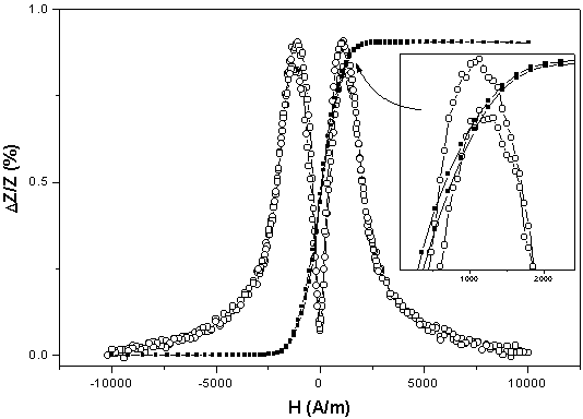
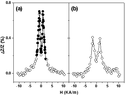
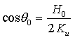
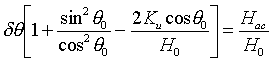
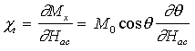
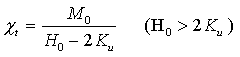
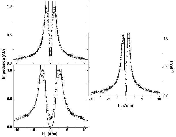
When a magnetic material carrying a low intensity, high frequency (up to 100MHz) alternating current is subjected to an external magnetic field, it exhibits a sharp change in its electrical impedance as shown in Figure 6.1a. This effect is known as the magneto impedance (MI) or the giant magneto impedance (GMI) effect. The external magnetic field is generally applied along the direction of the current flow as shown Figure 6.1b. The two MI curves shown in Figure 6.1a have been labelled as having been obtained at a low and high frequency. It can be seen from these two curves that the frequency of the applied current also has an effect on the form of the MI curve. The changes in the impedance are a consequence of changes in the interaction between the magnetisation of the material and the alternating magnetic field generated by the current. These changes occur due to the externally applied magnetic field. The key to understanding the MI effect is the effective permeability (meff) or effective susceptibility (ceff) [meff=ceff + 1] of the magnetic material. The magnetic field dependence of the impedance is controlled by the ability of the magnetisation to respond to the magnetic field generated by the current. This is governed by the effective susceptibility of the material in the direction of the field produced by the current. The application of the external field simply alters this effective susceptibility, which leads to the changes in the impedance. The impedance maxima shown in Figure 6.1a correspond to a maximum in the effective susceptibility. For the impedance curve obtained at low frequency, the effective susceptibility is a maximum when no external field exists, but decreases on the application of a field. This is not the case for the curve obtained at the higher frequency. Here the effective susceptibility increases to a maximum on the application of a small applied field, before decreasing with further increases of the field. The effective susceptibility is, in each case, influenced by two different magnetisation processes. The effective susceptibility in the low frequency case is dominated by reversible domain wall movement , whereas in the high frequency case, it is dominated by
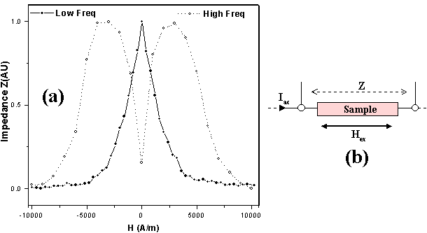
Figure 6.1: (a) Typical MI curves obtained from a FeSiBC film at two different current frequencies (labelled as low and high) as a function of applied magnetic field. Note the two curves have been normalised. (b) Illustration of basic impedance measurement.
| Growth and study of magnetostrictive FeSiBC thin films, for device applications, Mannan Ali (1999) | 131 | |
|---|---|---|
| (Online Copy) |
| Email:Mannan.Ali@physics.org | Chapter 6: Magneto Impedance investigation |
|---|---|
| Web: http://members.xoom.com/MannansZone/thesis.html |
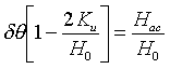
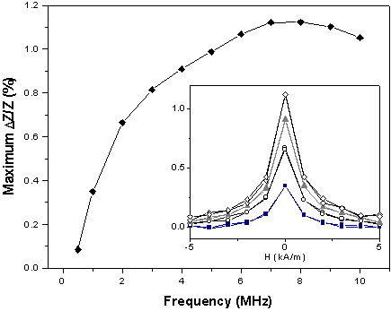
domain rotation (rotation of the magnetisation). For the high frequency MI curve, the two maxima can correspond to the anisotropy field of the sample obtained along the length of the sample. At sufficiently high frequencies, the skin effect (see below) can dramatically effect the impedance of the material, which is also dependent on the effective susceptibility. It is therefore possible to separate the MI effect at high and low frequencies.
It is generally accepted that when one refers to the giant magneto impedance (GMI) effect, it usually means that a skin effect is present which gives rise to much larger impedance changes. Whereas at low frequencies, where the influence of the skin depth is weak or non-existent, it is termed the MI effect, or more correctly the magneto inductive effect.
6.2.1 Low frequency limit
At relatively low frequencies, where the influence of the skin effect is negligible, the MI effect is due to changes in the reactance. In this situation the alternating current generates a magnetic driving field, which causes domain wall movement (oscillation), which in turn dominates the effective susceptibility. The changing magnetisation induces an additional voltage contribution, VL, which adds to the ohmic voltage due to the current [Mohri et al (1992), Velazquez et al (1994)].
 | (6.1) |
This additional induced voltage is termed the magneto-inductive voltage. The larger the effective susceptibility, the larger will be the change in the magneto-inductive voltage. On application of an external magnetic field, the changing magnetisation due to domain wall movement is suppressed and the magnetisation is rotated towards the applied field. This has the effect of decreasing the effective susceptibility, since the component of magnetisation which can interact with the alternating magnetic field generated by the current has been reduced. This leads to a fall in the magneto-inductive voltage, giving rise to the magnetic dependence of the impedance. This type of MI effect is relatively small compared to the GMI effect; the largest effect is found in cobalt based amorphous wires [Mohri et al (1992)].
| Growth and study of magnetostrictive FeSiBC thin films, for device applications, Mannan Ali (1999) | 132 | |
|---|---|---|
| (Online Copy) |
| Email:Mannan.Ali@physics.org | Chapter 6: Magneto Impedance investigation |
|---|---|
| Web: http://members.xoom.com/MannansZone/thesis.html |
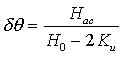
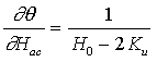
6.2.2 High Frequency limit (<100MHz)
The GMI effect has been explained in terms of classical electrodynamics [Beach et al (1994), Panina et al (1994)] as an interaction between the magnetic field created by the current and the magnetisation. At high frequencies the GMI effect is mainly due to changes in the resistive component of the impedance, since it is dominated by the skin effect. This causes the current to flow near the surface of the material, reducing the effective cross-sectional area of the material, leading to an increase in the resistive component of the impedance.
A mathematical description of the skin effect has been obtained from classical electrodynamics. For a conductor carrying a sinusoidal alternating current, the penetration or skin depth, d, is given by the well known expression
 | (6.2) |
where f is the frequency of the current, r is the resistively of the material, and ceff is the susceptibility. The susceptibility is the effective susceptibility in the case of GMI effect. It has been shown that for a thin film the impedance Z is related to the skin depth through the following expression [Panina et al (1995)]
 | (6.3) |
where Rdc is the dc resistance, and t the thickness of the conductor. It follows from expressions (6.2) and (6.3), that the impedance of a magnetic conductor again is dependent upon the effective susceptibility, through the skin depth. Here the effective susceptibility arises from two contributions: domain wall movement and oscillation of the domain magnetisation. At low frequencies, the domain wall movement dominates the susceptibility, whereas at higher frequencies the domain wall movement is strongly damped by microscopic eddy currents [Panina et al (1996)], and the magnetisation rotation contribution becomes dominant. Generally, this process results in a complex effective susceptibility [Panina et al (1996)]. The damping of the domain wall movement at high frequencies reduces the hysteresis effect, which is generally the source of the magnetic hysteresis. For successful sensor applications, it is vital that no hysteresis is present and therefore magnetisation rotation is usually preferable.
| Growth and study of magnetostrictive FeSiBC thin films, for device applications, Mannan Ali (1999) | 133 | |
|---|---|---|
| (Online Copy) |
| Email:Mannan.Ali@physics.org | Chapter 6: Magneto Impedance investigation |
|---|---|
| Web: http://members.xoom.com/MannansZone/thesis.html |
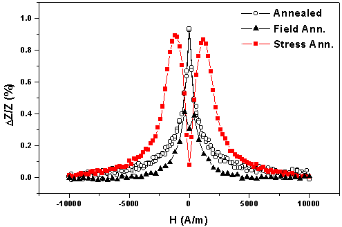
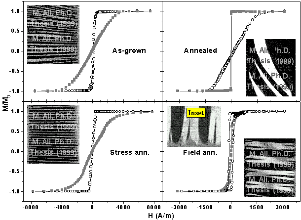
6.3 Domain structure and magnetostriction
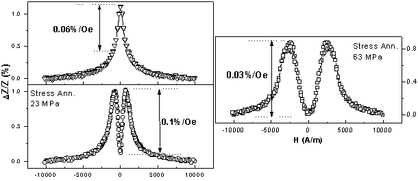
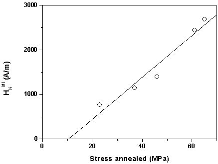
From the description of the MI effect so far, it is clear that the effect is controlled by the effective susceptibility. The magnitude of the susceptibility is controlled by the magnetic anisotropy of the material. For amorphous materials the intrinsic magnetic anisotropy is usually very small, and generally the magnetic anisotropy is extrinsically induced. This could be due to structural defects, strains/stresses introduced during the production of the material, or that of post production heat treatments, such as magnetic field annealing. Typically, the magnetic anisotropy for melt spun ribbons and wires is dominated by the stresses induced by the melt-spinning process. This is usually also the case with sputter deposited magnetic thin films, but not always, as shown by the radially induced magnetic anisotropy in the FeSiBC films discussed in Chapter 5, where it is inferred that the stresses induced during the deposition were negligible. It has been shown in Chapter 5, that the magnetic anisotropy, and therefore the domain structure, can be extrinsically controlled by various heat treatments. To obtain a significant MI effect, it has been generally found by many authors that the material should possess a domain structure in which the domain walls are perpendicular to the current direction. This ensures that the oscillating field generated by the current lies in an easy axis for the magnetisation. This should therefore maximise the effective susceptibility of the system.
There have been numerous investigations [Panina et al (1996), Tejedor et al (1996), Rao et al (1994)] of how the domain structure influences the MI effect. The nature of the magnetic anisotropy has been found to be especially critical in the case of amorphous wires [Costa-Kramer et al (1995), Panina et al (1996)]. Depending upon the sign of the magnetostriction, the amorphous wires which are produced by ejecting the melt into a continuous flow of rotating water, solidifies rapidly developing mainly a tensile radial stress distribution. This leads to two different domain structures being induced in the wire (Fig. 6.2). It is now generally accepted that the domain structures which result for the as-cast wires are
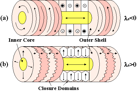
Figure 6.2: A simplified illustration of the domain structure for (a) negative magnetostriction, and (b) positive magnetostriction in amorphous melt-spun wires [Squire et al (1994)] of circular cross-section. The magnetoelastic coupling produces two different magnetic anisotropies, where the circumferential anisotropy (a) is more favourable than the radial (b) anisotropy for the MI effect in a circular wire.
| Growth and study of magnetostrictive FeSiBC thin films, for device applications, Mannan Ali (1999) | 134 | |
|---|---|---|
| (Online Copy) |
| Email:Mannan.Ali@physics.org | Chapter 6: Magneto Impedance investigation |
|---|---|
| Web: http://members.xoom.com/MannansZone/thesis.html |
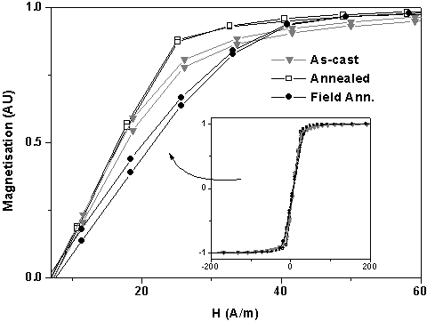
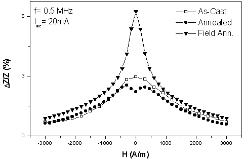
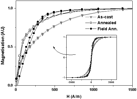
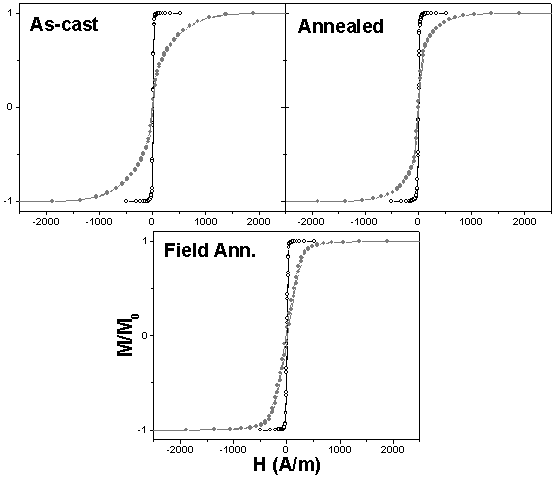
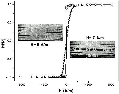
associated with the coupling between the magnetostriction and the stresses induced by the rapid quenching process. For both positive and negative magnetostrictive wires, the domain structure consists of essentially two regions as shown in Figure 6.2. The core region for the two wires is a single domain, with the magnetisation running along the length of the wire, and the outer region is a multi-domain structure, where the magnetisation is oriented radially for a positively magnetostrictive wire (moments lie along the stress direction), and circumferentially for a negatively magnetostrictive wire. The magnetic field generated by the alternating current is of a solenoidal form, and one would therefore expect to see a much greater MI effect in the case of the amorphous wires which have a circumferential domain structure (Fig. 6.2a), compared to that of the radial domain structure (Fig. 6.2b). Experimentally this has been found to be the case by many authors, and this partly explains why the Co based amorphous wires show the greatest effect, because the negative magnetostriction induces a favourable magnetoelastic anisotropy. Also the Co based materials have much lower anisotropy constant giving them a larger effective susceptibility. A recent investigation of the MI effect on FeSiB amorphous wires by Takemura et al (1996) has shown that, by lightly annealing the amorphous wires, the radial domain structure (Fig. 6.2b) of the as-cast wire weakens, and gives way to a circumferential domain structure; this is due to surface crystallisation. This leads to an increase in the MI effect, which has also been reported by Atkinson et al (1995), and highlights the importance of the domain structure on the MI effect. It is only the Co based amorphous wires which exhibit nearly zero magnetostriction which show the largest MI effect. Not only does the sign of the magnetostriction control the type of magnetic anisotropy induced, but the magnitude of the magnetostriction also influences how large a coupling there is between the magnetisation and the stresses. Too large a coupling would reduce the effective susceptibility, because of the larger induced magnetoelastic anisotropy. It is generally found that the nearly zero magnetostrictive materials are magnetically much softer (smaller coercive fields < 1A/m) as compared to those materials which have larger magnetostriction values, but the magnetostriction coupling is sufficient to induce a well defined magnetoelastic anisotropy. The same principles also apply to ribbons and thin films, where a uniaxial anisotropy of low magnitude is usually found to produce the maximum MI effect.
| Growth and study of magnetostrictive FeSiBC thin films, for device applications, Mannan Ali (1999) | 135 | |
|---|---|---|
| (Online Copy) |
| Email:Mannan.Ali@physics.org | Chapter 6: Magneto Impedance investigation |
|---|---|
| Web: http://members.xoom.com/MannansZone/thesis.html |
6.4 Sample preparation
The objective of this preliminary study into the MI effect, is to ascertain the potential use of thin films for MI sensors, and to correlate the magnetic properties with that of the impedance responses.
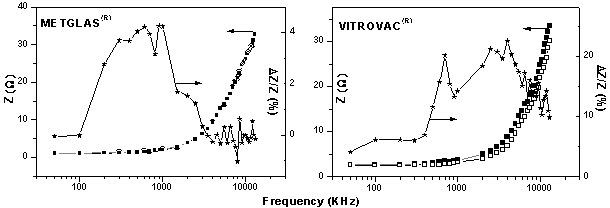
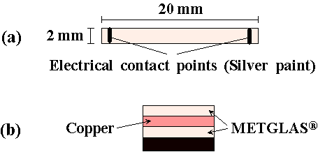
The experimental work carried out on the CoFeB thin films was a collaboration with David Garcia who was based at the Instituto de Magnetismo Aplicado in Madrid, under the Acciones Integradas program (HB95-0013). Two different compositions of magnetic thin films were investigated: FeSiBC films which were positively magnetostrictive, and CoFeB films which exhibited a slightly negative magnetostriction. The FeSiBC films were grown by RF magnetron sputter deposition at Sheffield, whereas the CoFeB thin films were in grown Madrid also by RF magnetron sputter deposition. The sputtering system used in Madrid is similar to the system described in Chapter 3. The CoFeB films were grown onto glass substrates from a solid, 20 mm thick target of composition Co76Fe4B20. The base pressure was in the range of 10-6 mTor, and the films were deposited at an argon pressure of 5´10-3 mTorr at a sputtering power of 300 W. The FeSiBC films were deposited using a sputtering power of 75 W at 4 mTorr of argon onto both glass and silicon substrates. The large difference in sputtering power is due the very thick CoFeB target which dilutes the magnetron effect, and a much higher power is therefore needed to obtain a reasonable sputtering rate. The amorphous nature of the two types of films was confirmed by X-ray diffraction q-2q scans using Cu Ka radiation. The thickness of the single layered films ranged from 0.5 mm to 4 mm, whereas the thickness of the copper layer (see later for significance of the copper layer) used in the layered films ranged from 0.15 mm to 2 mm. The copper layer was deposited from a 5mm solid target which had purity of 99.99% using the same sputtering parameters as for the FeSiBC layers. The planar dimensions of the patterned films were controlled by two methods: the first method was by cutting the deposited films grown on the silicon or glass substrates using a conventional diamond tip scribe, and the second method involved photolithography techniques as described in Section 3.6. The patterned film structures which were obtained by photolithography techniques ensured that a sharp, geometrical definition was obtained. This also prevented the thicker films from suffering from any micro-tears from the breaking procedure which could give rise to edge effects. The magnetic anisotropy of the samples as controlled by stress annealing, as described in Section 5.8.3, and also by a number of conventional heat treatments, which will become apparent during the discussion of the results. The magnetic properties of the FeSiBC films were determined using MOKE (Chapter 2), with both point hysteresis loops and domain imaging. Bulk measurements were also made using the inductive magnetometer (MH-looper see Section 3.2). The magnetic measurements of the Co based films were carried out at Madrid where similar magnetic measurements were taken. The MI measurements were carried out in Madrid using an automated system which has been described in Section 3.5. Measurements were also performed on METGLAS® 2605SC ribbon strips which had been carefully sliced from the central portion of the target material, along with a number of VITROVAC® 6025 ribbon samples. Electrical contacts to all samples were made via high purity copper thin copper wires which were attached to the samples using silver paint. The silver paint was allowed to dry for 24 hours to ensure good electrical contact.
| Growth and study of magnetostrictive FeSiBC thin films, for device applications, Mannan Ali (1999) | 136 | |
|---|---|---|
| (Online Copy) |

![Layered films [Morikawa et al (1997)]](images/img6_25.gif)


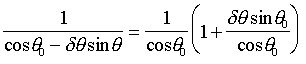
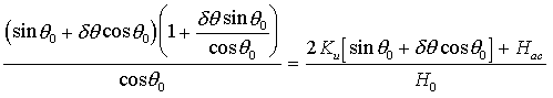
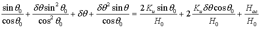
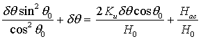
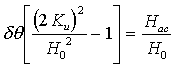
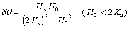
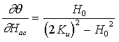
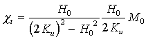
 and neglecting the