4.0 Thin Film Deposition The process of sputter deposition for the production of thin films in an increasing number of applications has increased widely in popularity. This is due to its ease of operation, accurate control of the growth rate (thickness), excellent film adhesion and a high degree of reproducibility of the deposited films. This chapter is concerned with the deposition and optimisation of the magnetic properties of amorphous FeSiBC thin films which have been sputtered deposited from METGLAS® 2605SC (Fe81Si3.5B13.5C2) ribbon targets, which were obtained from Allied Signal. The objective of this study was to obtain films which exhibited similar magnetic properties to those of the ribbon material. The results and findings presented here were obtained using radio frequency (RF) magnetron sputter deposition. An overview of sputter deposition of thin films is also presented, in order to highlight the problems of which one needs to be aware in the deposition of amorphous thin films, along with their general properties. 4.1 Introduction Since it was first discovered that melt-spun, amorphous, transition metal-metalloid alloys had excellent soft magnetic properties, there has been a tremendous amount of work done on these materials with a view to optimising their magnetic properties. The properties for Fe, Co and Ni based amorphous melt-spun alloys has been extensively documented [Luborsky (1980)], and commercial organisations such as Allied-Signal and Vacuumschmelze now produce a large range of melt-spun alloys. These are used in a wide variety of modern electrical and electronic applications. See Ref. List (4.1) for further information on types of applications where magnetic materials are used. Because of their soft magnetic properties melt-spun materials in the form of ribbons and wires (see Chapter 6) have also been exploited as stress and field sensors [Lenz (1990)]. Despite the wide availability of such materials in ribbon or wire form, in their current form they still have a number of disadvantages for modern sensor applications. Generally, the as-cast, melt-spun ribbons suffer from random residual stresses induced during the production stage. This has the effect of degrading the magnetic properties, especially if the material has a large magnetostriction, which is needed for stress-based sensors. This can lead to complex, random domain structures, which complicates both the understanding of the magnetisation process within the material and the output from the sensor itself. Ideally, for stress-based sensors, the domain structure should be orientated perpendicular to the direction of the applied stress to maximise the magnetoelastic effect (ls>0), or, in the instance of magneto impedance sensors, perpendicular to the applied current (see MI). This problem is overcome by annealing the ribbons in a magnetic field; this reduces the as-cast, random, residual stresses and induces a uniaxial domain structure. In many instances, the ribbon material is usually bonded to a rigid surface, depending on the type of sensor (i.e. Cantilever type sensor [Mitchell et al (1986)]), which can induce extrinsic random stresses because of distortions introduced when the adhesive dries; this can alter the optimised domain structure previously induced by field annealing. The annealing of some
![]() ![]()
ribbons, such as the METGLAS® 2605SC ribbon used in this thesis as the target material, has the undesirable effect of degrading the ductility. In most instances, this not a problem, since the ribbon is usually bonded to a rigid surface, where the stresses transmitted from the rigid surface to the ribbon are relatively small. However, advances in technology generally mean some form of miniaturisation. Sensors are now being integrated and microfabricated onto commercially important substrates such as silicon and gallium arsenide in such ways that they are compatible with conventional microelectronic fabrication. This allows all the components required for the sensor device to operate to be fabricated on the one substrate. To keep in step with such developing technologies, the potential of these amorphous alloys are now being exploited in thin film magnetic sensors. Magnetic thin films also allow the fabrication of more exotic, three dimensional structural sensors, such as membranes [Karl et al (1999)] and cantilevers [Karl et al (1999a)] on a micron scale. Ribbon materials in their current form would be difficult to incorporate into such small sensor elements. By no means does this mean that magnetic thin films do not pose any problems of their own. The magnetic and structural properties of thin films are strongly dependent upon the deposition process and the parameters under which the film is deposited. Sputtering and evaporation techniques are the two common methods of preparing amorphous magnetic thin films, with the former being the most popular of the two. To achieve device quality thin films with similar magnetic properties to that of the ribbon materials, three main requirements need to be fulfilled: the composition of the film needs to be correct to maintain the required magnetic properties, the microstructure needs be amorphous and, if possible, a uniaxial anisotropy needs to be induced in a given direction. Controlling the composition of the depositing film by vapour deposition is a very difficult process, because of the widely differing melting points and vapour pressures for the different elements. However, sputter deposition tends to preserve the composition of the depositing film [Elliot (1984)] as that of the target alloy, since the sputtering rates tend to vary less widely and this therefore is the more popular method of the two. The very high cooling rates generally ensure the structures of the deposited films are amorphous under most conditions or, at worst, nanocrystalline. The magnetic anisotropy and the methods of controlling the anisotropy in thin films is discussed in the following chapter. 4.2 Parameters which effect sputter deposited films Sputter deposition is a complex process where there are combinations of sputtering parameters which influence both the magnetic and structural properties of the depositing film. Generally, it is found that one set of sputtering parameters on a given sputtering system cannot be transferred to another system to deposit films with the same magnetic and structural properties. This illustrates how sensitive the films are to the sputtering parameters (see below). It also explains why one finds that similar magnetic films deposited by different researchers are performed under different sputtering conditions. Careful control of the sputtering parameters is essential to prevent the films suffering from residual stresses and columnar growth (see below) which can severely affect both the magnetic and structural properties. The
![]() ![]()
stresses which deposited films suffer from arise from two contributions: the extrinsic stresses which are brought about by differing thermal expansion coefficients of the film and substrate and the intrinsic stresses which are a result of the sputtering process itself and are discussed below. 4.2.1 Pressure: The pressure of the sputtering gas is very important, not only does it provide the inert gas ions needed for the sputtering process of the target, but it also acts as a moderator for the ejected atoms from the target. By careful control of the pressure, one can influence both the structural and magnetic properties of the film. At low pressures, the sputtered and reflected neutral atoms have much higher energies than the plasma gas between the target and substrate and arrive at the substrate with super-thermal energies. The sputtered atoms in this situation have a high surface mobility at the substrate. At higher sputtering pressures, the sputtered and reflected neutral atoms, are thermalised [Somekh (1984)] by the plasma gas, due to the increased number of collisions before arriving at the substrate. As a consequence, the sputtered atoms will have a lower surface mobility at the substrate. This will have a significant effect in the growth kinetics of the depositing film and is reflected in the magnetic and structural properties. It is therefore essential that the sputtering pressure is carefully investigated to obtain the optimum magnetic and structural properties. 
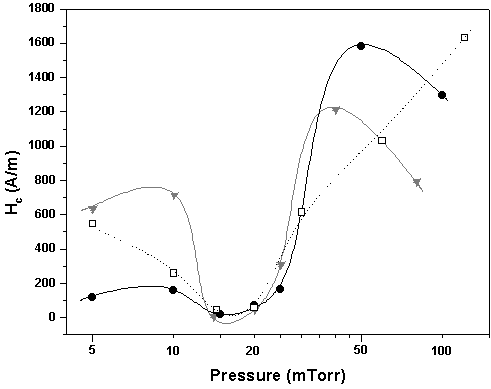
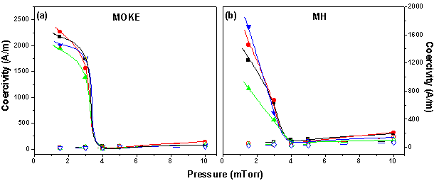
There have been numerous studies exploring the effects of pressure on sputter deposited films, and it is well established that the pressure has a significant effect on the magnetic properties, mainly through stress [Ref. List (4.2)] and columnar growth [Shimada et al (1981), Leamy et al (1979)]. The as-deposited films tend to suffer from residual stresses if the effects of pressure have not been accounted 
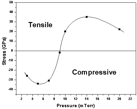
Figure 4.1: Stress dependence as function of pressure for Co-based films obtained by RF sputter deposition. [Data obtained from Materne et al (1988)].
![]() ![]()
for. This generally changes from being a compressive to a tensile stress as the sputtering pressure is increased. An example of such an effect is shown in Figure 4.1, where an investigation of stress in sputter deposited low magnetostrictive Co-based films was performed by Materne et al (1988) as a function of pressure. At low argon pressures, the films were found to be under compressive stress, whilst at higher pressures the stress was found to be tensile. A transition region at approximately 9mTorr existed where the stress changes sign, and the as-deposited films were found to be in a ‘stress free’ state; this also corresponded to the lowest values of the coercive field (15-30 A/m) as a function of pressure. It is the general consensus that at low pressures, the high surface mobility of the sputtered atoms promotes the formation of dense films which are under compressive stress. The compressive stress is inferred to be due to argon entrapment and lattice distortion caused by energetic incident particles. At higher pressures, the sputtered atoms are less energetic because of the increased scattering. This lowers the surface mobility of the sputtered atoms; it also causes the sputtered atoms to arrive at the substrate at more oblique angles, because of the increased scattering. This can result in the films having a columnar morphology, which induces a tensile stress in the film. The columnar growth is a result of the self-shadowing of the incident atoms by those already incorporated into the growing film [Leamy et al (1979)]. This is obviously controlled by the surface mobility of the sputtered atoms, which in turn is related to the incident energy of the sputtered atoms. As the pressure is further increased to even higher pressures, there is a reduction in tensile stress (Fig. 4.1) in the films, because of the more distinct columnar structure. The more open, columnar morphology is said to prevent the ease with which the stress can be transmitted between the columns [Hudson et al (1996)]. It has also been suggested that the tensile stress at higher pressures may be due to oxygen contamination, since there seems to be a strong correlation between oxygen incorporation and columnar growth morphology developed at high pressures [Leamy et al (1978,1979), Materne et al (1988)]. However, the effect of oxygen on stress is not clearly understood, since there have also been reports that at high pressures, oxygen incorporation leads to compressive stresses [Hoffman (1976), Hudson et al (1996)]. Similar trends due to pressure also occur on other magnetic systems such as FeCoB [Shimada et al (1981)], and FeSiB [Naoe et al (1979)] thin films which have been sputtered deposited. It should be noted that intrinsic stress from sputtering is not only confined to magnetic films and can occur in any sputter 
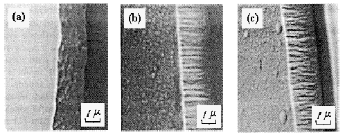
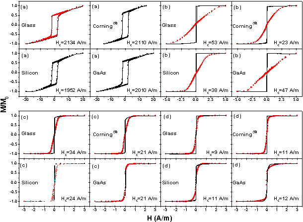
Figure 4.2: FeCoB films obtained by RF sputter deposition. Scanning electron microscopy of fractured edges of films deposited at (a) 3mTorr, (b) 50mTorr, and (c) 150mTorr indicating the development of columnar morphology at high pressures. [Data obtained from Shimada et al (1981)].
![]() ![]()
deposited systems, for example copper [Craig et al (1981)] or tungsten [Vink et al (1993)] films. The morphology of thin films has been summarised by Thornton et al (1974) and Craig et al (1981), where they describe various structure zones, depending on the sputtering pressure and substrate temperature. They infer that the stress and structure of the film is related to the energy of the bombarding particles at the substrate during the sputter deposition. Dense non-columnar films are obtained when the impinging particles (sputtered and reflected neutrals) have high kinetic energies (low pressures), and a distinct columnar texture is developed at low particle energies (high pressures). This is shown in Figure 4.2, where FeCoB thin films were sputter deposited by Shimada et al (1981) at various argon pressures to investigate the magnetic and structural properties. It was found that the columnar texture only appeared at high sputtering pressures (>50mTorr), and the films deposited at low argon pressures (<10mTorr) showed no characteristic structure. These results are in agreement with other studies [Naoe et al (1979), Materne et al (1988)] which also have found that films deposited at low pressures do not have any characteristic columnar morphology. It is well accepted that to obtain good magnetic amorphous films with a high saturation magnetisation and a low coercive field, the sputtering conditions need to be carefully chosen to suppress the formation of columnar growth, which is found to be unfavourable for the soft magnetic properties. In most sputtering systems, the sputtering gas, usually argon, is allowed to flow continuously through the chamber at a constant pressure; this helps with the removal of any out-gassing impurities which could otherwise build up within the chamber and be incorporated into the depositing film. It is important that the gas flow-rate is not to excessive, since this can lead to the existence of pressure gradients within the chamber and cause non-uniform sputtering of the target, which can be reflected in a non-uniform film thickness. 4.2.2 Target-substrate separation: The separation between the target-substrate has a similar effect, as does the sputtering pressure on the growth kinetics. Increasing the separation between the target-substrate has the effect of lowering the mobility of the atoms at the substrate; the reverse is true when the separation between the target-substrate is decreased. This assumes that the sputtering power does not have total dominance over the energy of the particles. A number of studies [Hudson et al (1992,1996)] have been performed to investigate the relationship between the pressure and target-substrate separation. It has been found by Hudson et al that a relationship exists between the pressure P, the target-substrate separation, d, and the stress found in the sputter deposited films. It was reported that films deposited at low values of the product, Pd, produced films which were under a compressive state of stress, whereas films deposited at high values of the product, Pd, were under a state of tensile stress. It was inferred that the stresses present in the films were related to the energy of the bombarding particles, as discussed above for pressure.
![]() ![]()
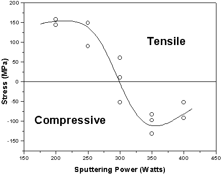
Figure 4.3: Stress dependence as function of sputtering power for tungsten films obtained by sputter deposition. [Data obtained from Wagner et al (1974)]. 4.2.3 Sputtering Power: The sputtering power also has a similar effect to that of the pressure as described above. Figure 4.3 shows the variation in stress for sputter deposited films as the sputtering power is increased. It can be seen that, at low sputtering powers, the film is in a state of tensile stress, whereas the stress state of the films becomes compressive at higher powers. This is due to the increasing kinetic energies of the particles and hence surface mobility. The deposition rate increases linearly with increasing power but, from Figures 4.1 and 4.3, it is clear that to obtain stress-free films, the deposition rate is somewhat restricted by these parameters. The sputtering rate can be increased by use of a magnetron (Section 3.1.3) in conjunction with the target. This produces a denser plasma at the target surface, which increases the deposition rate without increasing the sputtering power. However, the use of low sputtering powers ensures that the system, target and substrate temperature rises are minimised. 4.2.4 Substrate temperature: The substrate temperature is very important in controlling the magnetic and structural properties of the depositing film. In the situation where there is a large difference in the thermal expansion coefficients of the depositing film and substrate, it is essential that the substrate temperature is maintained close to room temperature. This will minimise the stresses induced in the film after the deposition, as the film and substrate contract differently on cooling. The temperature of the substrate will also influence the surface mobility of the sputtered atoms, which will therefore control the structure and intrinsic stresses due to the sputtering process. The substrates are usually water-cooled through the substrate platter, but there can still be a significant increase in the temperature of the surface of the substrate, depending on the sputtering conditions, especially if the substrates are poor conductors such as glass, or they are very thick. The low sputtering pressures used during the deposition also means the thermal contact between the substrate and platter is not ideal. The increase in the surface temperature is mainly due to energetic sputtered atoms and secondary electron bombardment of the substrate. Secondary electron bombardment is significantly minimised on magnetron sputtering systems, where the electrons are captured by the magnetic field. Ounadjela et al (1987) have demonstrated that, by applying a DC magnetic field parallel to the substrate at the substrate platter, it is
![]() ![]() | ||||||||||||||||||||||||||||||||||||||||||||||||||||||||
possible to reduce the substrate temperature by 1500C in RF sputter deposition systems. It was inferred that this was due to the reduction of secondary electron bombardment. The only disadvantage with this method is that the magnetic anisotropy of the film is essentially controlled by the applied field. 4.2.5 Nature of substrate: The structure and surface condition of the substrate is very important in determining the magnetic and structural properties of the film. It is important to be aware of the thermal expansion coefficients of the substrate and the depositing film. Large differences in the expansion coefficients can cause extrinsic stresses to be introduced into the film, which can influence the magnetic properties such as the anisotropy via the magnetostriction. Any texturing of the substrate can influence texture into the depositing film. The first few layers of the depositing film are expected to conform with the texture, contours and imperfections of the substrate. For thin films, the magnetic properties may be sensitive to scratches or imperfections in the substrate, as will the surface mobility of the atoms since they will need to overcome these obstacles to remain mobile. In the case of amorphous films, the films are deposited onto smooth, amorphous substrates such as glass, or silicon/gallium arsenide substrates which have an amorphous oxide layer. This prevents any possible texturing effects being induced from the substrate. The cleanliness of the substrate surface is important to prevent contamination of the films from oily/greasy residues, which can also cause the films to de-laminate. A number of methods are used to remove surface dust and contamination from the substrates: [1] Substrates are physically cleaned using degreasing solutions such as isopropanol, using fibre-free cloths in conjunction with dry nitrogen gas. [2] Ultrasonic agitation in an isopropanol bath. [3] Ion bombardment of the substrates prior to deposition of the film. This is an effective method of removing any surface contamination. This process is also referred to as pre-sputtering. However, care must be taken to ensure that the surfaces of the substrates do not become roughened in the process, which can affect the magnetic properties by introducing pinning sites for domain walls. The pre-sputter cleaning also increases the temperature of the substrate significantly, compared to the temperature during the deposition. If the deposition of the film commences immediately on completion of the sputter clean, this can cause the first layers of the film to be deposited onto a substrate at a much higher temperature, compared to the rest of the depositing film, thereby placing the lower layers of the film under a compressive state of stress as the substrate equilibrates to the deposition temperature. The cleaning procedure adopted is dependent upon the type of substrate, and whether or not there are any fabricated devices on the substrates which could be affected. Another important point about the substrates that one should be aware of, is their thermal and electrical properties. Amorphous films deposited onto good thermal conductors, can be remarkably different to those deposited onto an insulating substrate under identical sputtering conditions. This is usually a result of the much cooler substrate surface, which will affect the surface mobility of the sputtered atoms. It should be remembered that insulating substrates can only be sputter cleaned by RF sputtering, unless an ion gun is added to other types of sputtering systems.
![]() ![]()
Figure 4.4: Target arrangements used in the deposition of metalloid films. 4.2.6 Target Composition: The nominal film composition and uniformity of the magnetic properties are determined by the target. It is therefore important that the composition of the target is correct and uniform throughout the target. In most instances, the target consists of a solid disc of the correct composition which has been carefully cast. Other methods involve placing small, circular pieces of various pure elements onto the main circular target [Naoe et al (1979)] or embedding circular pieces [Shimada et al (1979)] into the target as shown in Figure 4.4 at regular intervals. By varying the number of pieces it is possible to control the composition of the film. In more elaborate systems, to overcome the problems with non-uniform compositional targets, the substrate platter is slowly rotated [Aboaf et al (1978)] to ensure the composition is uniform throughout the film. 4.2.7 Substrate Biasing: Substrate biasing is usually achieved by applying a negative, or positive, DC potential to the substrate platter. Applying a negative bias to the substrate during the deposition will cause the depositing film to suffer from a bombardment of positive gas ions and is referred to as bias sputtering. This can have the effect of increasing the temperature of the substrate and hence surface mobility of the sputtered atoms. The process can also lead to the incorporation of sputtering gas, giving rise to compressive stresses and it can also be used to control the final composition of the film. A positive bias is applied to minimise the bombardment of the film from positive gas ions, but this can have the effect of increasing secondary electron bombardment of the substrate platter and oxygen incorporation. The effects of substrate biasing have shown that a negative bias produces compressive stresses, whereas a positive bias produces tensile stresses in thin films [Ohkoshi et al (1985), Leamy et al (1979), Wagner et al (1974)]. 4.3 Magnetic properties of thin films It has been confirmed by many researchers [Ref. List (4.3 & 4.4)] that it is possible to deposit amorphous magnetostrictive thin films, which have excellent magnetic properties. In most cases, it has been highlighted that the sputtering conditions have a significant effect on the magnetic properties and structure. The magnetic properties in particular have been investigated as a function of sputtering pressure [Ref. List (4.4)], since it is a parameter which is easily controlled and does not generally influence the sputtering process apart from moderating the kinetic energies of the particles arriving at the substrate. Varying the sputtering power for example, increases the sputtering rate, the target temperature, the substrate temperature from the increased electron bombardment, together with the
![]() ![]()
kinetic energies of the sputtered and reflected particles arriving at the substrate. It is well established that the magnetic properties of deposited films are very sensitive to intrinsic stresses, which can severely affect the magnetic properties such as the coercive field and the anisotropy field. By careful control of the pressure, it has been shown that stresses in the deposited films can be minimised [Materne et al (1988)] to give low coercive field values. The effect of pressure on the coercive field is illustrated in Figure 4.5, for three Fe-based alloys. It can be seen that the coercivity is a strong function of pressure, and clear minima in the coercivity exist in the region of 15-20 mTorr for these magnetic films. The changes in the coercivity are essentially due to variations in the induced stresses in the deposited films as discussed previously. It should be pointed out that Kazama and Heiman et al (1979) have ruled out the possibility that the variation is a result of any compositional changes, since no such changes were found for the FeSiB and FeCCrP films, which displayed similar coercivity trends to the FeC films and which did show some variation in composition as a function of pressure. It was also shown that an obvious correlation existed between the coercivity and the anisotropy field, which seemed to imply that the variations were a consequence of stress. This was confirmed by annealing the samples, which exhibited high coercive (>400A/m) and anisotropy (>32kA/m) fields, to relieve the induced stresses present. The corresponding values for the coercive and anisotropy fields were found to be less than 80A/m and 7kA/m respectively. The conclusion that stress was the dominant factor in controlling the magnetic properties was further strengthened by the deposition of CoFeB thin films, which exhibit zero magnetostriction (ls»0 ppm). The deposited films displayed coercive and anisotropy field values less than 80A/m, irrespective of the sputtering pressure. The magnetic properties of these films were not sensitive to the induced stresses because of the zero magnetostriction. The effects of stress are found to be more pronounced in highly magnetostrictive materials, than in the zero magnetostrictive materials; this is as one would expect. The pressures at which the soft magnetic properties are obtained usually corresponds to the films being in the most ‘stress free’ state. Figure 4.5: Coercive field dependence as function of sputtering pressure for films obtained by sputter deposition. Inverted triangles represent FeC (ls=15 ppm), open squares represent FeSiB (ls=20 ppm) and solid circles represent FeCrPC (ls=10 ppm) thin films. [Data obtained from Heiman et al (1979), Kazama et al (1979)].
![]() ![]()
As discussed earlier, the magnetic properties are dependent upon a number of sputtering parameters and it is important to fully investigate the effects of these parameters on the magnetic properties. Naoe et al (1982) have shown that optimising the sputtering pressure for one magnetic system does not necessarily imply that other magnetic systems will also produce soft magnetic properties at the same pressure. In the instances where stress is a dominant factor in highly magnetostrictive films, the magnetic anisotropy will be generally be determined by the sign (tensile or compressive) and magnitude of the stress present. It has been reported [Ref. List (4.5)] that the magnetisation in the as-deposited magnetostrictive amorphous films can be perpendicular to the plane of the film. This is usually the result of the intrinsic stresses which are induced during the sputtering process, coupling with the magnetisation via the magnetostriction. A perpendicular anisotropy will be induced in positively magnetostrictive films, if large bi-axial compressive stresses exist within the film. Tensile stresses will induce an in-plane magnetic anisotropy. The reverse is true for negatively magnetostrictive films where large bi-axial tensile stresses will result in the magnetisation lying out-of-plane. Heiman et al (1978) and Kazama et al (1978) have shown that the magnetic anisotropy for positively magnetostrictive films is indeed out-of-plane, and is the result of compressive stresses, since deposition of CoFeB (ls»0 ppm) films, resulted in an in-plane magnetic anisotropy. Similar results are also reported by Kobliska et al (1978). In both cases, the perpendicular anisotropy of the films could be transformed by appropriate annealing to relieve the residual stresses so that the magnetic anisotropy lay in the plane of the film. Perpendicular anisotropy can also be a consequence of columnar morphology, which can appear under certain sputtering conditions, mainly at high sputtering pressures as found by Materne et al (1988). Films of CoZrNb (ls=-0.6ppm) were found to posses perpendicular anisotropy at high pressures, where the residual stress was found to be of the tensile form, and the magnetisation was in-plane at low pressures where the stresses in the films were compressive (Fig. 4.1). This is the opposite to what has been discussed for positive magnetostrictive films. On annealing the films, it was found that the films deposited at low pressures, and which were initially in a compressive state, were now in a state of tensile stress, and the films deposited at high pressures were still in a state of tensile stress. The magnetic anisotropy of the films at low pressures was still in-plane and magnetic anisotropy of the films at high pressures was still perpendicular. This indicates that the perpendicular anisotropy at the higher argon pressures is not the result of stress, since all films were in a state of tensile stress after annealing. Scanning electron microscopy of the samples clearly indicated the formation of columnar morphology for films deposited at high pressures, which was absent in the films deposited at low pressures. It was therefore presumed that the columnar structure was the cause of the perpendicular anisotropy, due to shape anisotropy of the columnar structure. Similar findings have also been reported by Shimada et al (1982). It is well established that the composition of the bulk metal-metalloid amorphous ribbons generally does not deviate much from the 80% transition metal and 20% metalloid composition ratio [Luborsky et al (1979,1980,1980a)], where the optimum magnetic properties are found to occur. The wider compositional ranges possible from sputtering amorphous thin films has also been investigated, and it is
![]() ![]()
Table 4.1: Magnetic properties of Fe-based films obtained by sputter deposition. Table 4.1: Magnetic properties of Fe-based films obtained by sputter deposition. generally found that the best magnetic properties are attained at approximate ratios of 80% to 20% metal-metalloid composition. The as-deposited magnetic properties tend to suffer slightly from residual stresses, but appropriate annealing of the films has shown that the magnetic properties are quite comparable to similar compositions of amorphous ribbons. Coercive fields as low as 3 A/m and 4A/m have been obtained for F80B20 and Fe79B16C5 films respectively by Tsunashima et al (1981). A number of film compositions along with their magnetic properties are tabulated in Table 4.1. It is clear from the literature that it is possible to obtain amorphous films with magnetic properties which are comparable to those of the amorphous ribbons, as long the sputtering conditions have been carefully optimised. Annealing of the samples after the deposition can further improve the magnetic properties.
![]() ![]()
4.4 Results and Discussions 4.4.1 General findings The FeSiBC films were deposited from METGLAS® 2506SC ribbon targets obtained from Allied Signal using RF magnetron sputtering as described in Chapter 3. The compositions of the film are similar to that of the target material, which is known to display excellent magnetic properties. A number of problems were encountered at the start of the investigation, which had to be addressed. The main problem was the lack of reproducibility of the deposited films, at apparently identical sputtering conditions. It was found that the films had widely different magnetic properties (Hc, Hk) between consecutive runs. Pressure and power series displayed no obvious trends and they were found to be different every time they were performed. At this stage, the substrates being used were 1cm2 Corning® and standard glass pieces which were glued to a standard glass slide using a high vacuum compatible glue. The slide was then mounted to the substrate platter as shown in Figure 3.4a. For consistency the glass pieces were always glued in the same position. The substrates were cleaned as described in Section 3.1.3, and then sputter cleaned for 1 minute at 5mTorr at a sputtering power of 100W. The variations seen at the fixed power and pressure were obviously due to some other varying parameter, since these two parameters were monitored and found to be very stable during consecutive depositions. It was thought the pre-sputtering of the substrates could be one of the sources of the irreproducibility, since the process does cause the substrates to heat up substantially; also, it has been shown by Mattingley (1997) that the sputtering parameters need to be carefully optimised to ensure that the substrates are not over-etched such that the surfaces become roughened. This can lead to the introduction of pinning sites for domain walls and to inhomogeneous stresses being induced in the film. The pre-sputtering of substrates was stopped since it was not possible to ascertain, at the time, if the cleaning procedure was causing the surfaces of the substrates to be cleaned differently from consecutive depositions. In most instances, the substrates cannot be sputter cleaned if the film is being deposited on to a fabricated substrate containing sensor elements, and therefore soft magnetic properties would be needed without this process. The removal of the sputter cleaning procedure seemed to have no effect, and it was decided that the problem might lie in the actual glueing of the 1cm2 substrate pieces to the standard glass slides. It was thought that the glue was causing variations in the thermal contact between the 1cm2 substrate pieces and the glass slide. The changing temperature of the substrate surface will affect the magnetic properties of the film, because of the variations in the surface mobility of the atoms. Films were then deposited onto complete standard glass slides, which were clamped to the substrate platter. The films deposited on the glass slides revealed that the problem was not due to the glue, and it was at this stage that it was noticed that the shape and position of the plasma itself varied between consecutive runs. This indicated that there was an electrical problem with the sputtering system, mainly the earthing around the chamber. The grounded chamber and components within the chamber ensures that the plasma gas is confined over the target area and does not come into contact with any other surface within the chamber. Any deviations in the earthing will give rise to variations in the plasma kinetics. Tests revealed that earthing on the main chamber and the base of the chamber had become
![]() ![]() | ||||||||||||||||||||||||||||||||||||||||||||||||||||||||||||||||||||||||||||||||||||||||||||
insufficient for the RF environment being used. It was found that the spring earthing clips (see Fig. 3.2) which were positioned around the base of the chamber and which made electrical contact between the base and the main chamber had become defective, and it was no longer sufficient from the point of the RF being used. The two Viton seals essentially electrically isolate the main chamber walls from the rest of the machine (see Fig. 3.2), and these spring earthing clips ground the walls in conjunction with a high density conducting braid which is attached to a single point on the chamber wall. The earthing through the spring clips had become intermittent, as had the earthing to the target and substrate shutters within the chamber. The shutters were earthed through mechanical gears which had become defective because of wear. On rectifying these problems, it was found that the plasma discharge was visibly changed, and was essentially confined over the target. The inconsistency of the magnetic properties of the deposited films at fixed sputtering parameters was also cured. This illustrates how sensitive and complex the sputtering process can be to any sputtering parameter. 4.4.2 Substrate mounting It was found that clamping the glass slides to the substrate platter, as shown in Figure 3.4a, influenced the magnetic anisotropy of the deposited films. It is shown in the next chapter that it is possible to control the magnitude and direction of the magnetic anisotropy by stressing the slides by mechanical bending. Generally, the glass slides are not perfectly flat, and this therefore induced an uncontrollable amount of stress into the films, at random, when the slides were clamped to the substrate platter. To overcome this problem, the substrates were mounted using a picture frame holder (Fig. 3.4b) which ensured that no clamping forces which could induce any preferential anisotropy existed on the substrates. The holder also ensured the free movement of the substrates, which allowed for any thermal expansion of the substrates during the deposition of the films. It also ensured the consistent positioning of the substrates on the platter. 4.4.3 The effects of pressure A range of pressure and power investigations were performed, and it was found that films deposited above a sputtering power of 120W had inconsistent magnetic properties between consecutive growths; this was attributed to the high temperature of the substrate platter. It was not possible to monitor the temperature of the substrate platter during the deposition, but it was found that it was too hot to physically touch straight after the deposition of films at high powers (80-900C). The high temperatures cause the films to suffer from stresses as the film and substrate contract differently because of the difference in thermal expansion coefficients (FeSiBC=5.9ppm/0C glass=7ppm/0C) and also compressive stresses are induced due to the increased mobility of the sputtered atoms and argon incorporation. It was found that a sputtering power of 75W, produced films which were consistent as a function of pressure, and a reasonable deposition rate of ~5.5nm/min was attainable. More importantly the temperature of the substrate was also estimated to be between 40-1000C during the deposition at 75W; this was because of the significant decrease in heating from the plasma. This was ascertained by fixing 1cm2 glass pieces to
![]() ![]()
Figure 4.6: Pressure dependence on (a) standard glass slides and (b) 1cm2 Corning®. The solid squares represent the as-deposited films, the open circles represent the films after an anneal at 3900C for 1 hour. Both pressure series were performed at 75W, and the respective films thicknesses are 750nm and 330nm. (a) Data obtained using MOKE. (b) Data obtained using MH from 1cm2 pieces which were glued to a standard slide. a standard glass slide using wax which has a melting point of 400C and also by glueing 1cm2 glass pieces coated with photo-resist (see Section 3.6). It was found that the glass pieces attached with wax fell off within the first few seconds of the deposition, indicating that the temperature was above 400C, but the photo-resist was intact after the depositions, which implied that the temperature of the substrates was below 1000C. Prolonged heating of the photo-resist at approximately 1000C or above causes the resist to deteriorate -i.e. hard baked; the resist becomes more difficult to remove using a solvent [Karl (1998)]. The measured temperature of the substrate platter immediately (1min) after the deposition was 40-450C. Figure 4.6 shows the coercivity dependence of the FeSiBC films deposited at 75W as a function of argon pressure on glass slides and 1cm2 Corning® pieces. A clear minimum in the coercivity exists at 4-5mTorr and, as the argon pressure is decreased, there is a sudden increase in the coercivity, whereas there is a gentle increase in the coercivity with increasing pressure. The sudden increase in coercivity below 4mTorr is attributed to the large compressive stresses being induced in the depositing film, this is due to the increased kinetics of the sputtered and reflected particles at the substrate. The sign and the extent of the stress present was monitored by depositing films onto glass cantilevers 50x5x0.1mm3 which were firmly glued to the glass slides to ensure good thermal contact. If the film side of the cantilever, on removal, bent in a convex form, it indicated that the film was in a state of compressive stress during the deposition; a concave cantilever indicates tensile stresses. The cantilevers were removed by dissolving the glue in acetone. Cantilevers obtained below 4mTorr exhibited large compressive stresses, whereas the cantilevers obtained above 4mTorr appeared to be flat within the experimental limit. It was therefore difficult to determine if the stress was compressive or tensile above 4mTorr, since they appeared to be equally flat as shown in Figure 4.7. The dependence of the coercivity on stress is further strengthened by annealing the films to relieve the stresses induced during the deposition. In all cases, except films grown at 20mTorr, there was a reduction in the coercivity, which was also mirrored by the annealed cantilevers (Fig. 4.7). This indicates that the coercivity is dependent
![]() ![]()
Figure 4.7: Glass cantilevers deposited at 75W at the pressures indicted before and after stress relief. Images taken using a Zoom lens in conjunction with a CCD camera. The cantilevers were placed on a glass slide to observe the extent of the stress present by observing the deflection indicated below. No attempt was made in quantifying the stress using this crude method. Figure 4.8: Orthogonal MOKE loops obtained from a FeSiBC films deposited at 75 watts at the pressures indicated, for the as-deposited state and annealed state. Films were annealed at 3900C for 1 hour for stress relief. upon the stresses which are induced during the deposition process, as a function of pressure, as reported by other authors [Ref. List (4.4)]. Such large variations, cannot therefore, be a result of changes in the composition as a function of pressure as, shown by Mattingley (1997) and Heiman et al (1978), the compositional variations for these types of alloys are negligible over the pressure range investigated. The reduction in coercivity on annealing indicates that the high initial coercivity is unlikely to be due to the composition or crystallisation, since annealing does not change the composition, and it would induce further crystallisation on annealing, thus increasing the coercivity. The hysteresis loops for films
![]() ![]()
deposited on glass slides at 1.5, 4, 10, and 20mTorr are shown in Figure 4.8. The magnetic anisotropy in each of the deposited films is very different and it is clear that a uniaxial anisotropy appears to develop strongly in-plane as the sputtering pressure approaches 4mTorr. It should be noted that the anisotropy appears to be uniaxial because of the point hysteresis measurement, but it is shown, and discussed in the next chapter, that the films display a unique, radial magnetic anisotropy distribution [Ali et al (1998)] for films deposited at argon pressures between 4-15mTorr. This has been attributed to the residual field from the magnetron source. Below 4mTorr, the magnetic anisotropy appears to be isotropic in the plane and, from the cantilever measurements, it is known the films are under a state of high bi-axial compressive stress. The bi-axial compressive stress accounts for the isotropic in-plane hysteresis loops, since it is known that high compressive stresses in films can induce the magnetisation to lie out of the plane [Ref. List (4.2)]; this is due to the coupling between the stress and magnetostriction (ls=30ppm ). The annealing of the films deposited below 4mTorr demonstrates that the magnetic anisotropy and the initial coercivity are due to the compressive stresses, since the hysteresis loops for all samples deposited at 15mTorr or below display a similar in-plane magnetic anisotropy after annealing, which relieves the induced stresses. The MOKE hysteresis loops for the films grown at 20mTorr after annealing indicate that the perpendicular anisotropy does not decrease but, on the contrary increases, and therefore indicates the anisotropy and the increase in coercivity are not due to stress. Increases in the stress due to the annealing (thermal mismatch film/substrate) can be neglected because of other samples grown at lower pressures which were annealed at the same parameters. Materne et al (1988) have shown that films deposited at 20mTorr exhibit columnar growth; annealing the films increased both the coercivity and the anisotropy field. The possibility of the occurrence of columnar growth in the FeSiBC films deposited at 20mTorr was not verified at the time, since the results would be of no real interest to this investigation. The aim was to produce soft magnetic films, which would be useful for applications such as sensors. It is assumed the that perpendicular anisotropy is a consequence of some form of columnar growth. A similar trend is also observed for films deposited onto Corning® glass, where stress dominates the magnetic properties as discussed above. Examples of hysteresis loops on Corning® glass will be discussed later. 4.4.4 Substrate sputter-clean The effects of pre-sputtering glass and Corning® substrates was investigated using the parameters which were found to be suitable by Mattingley (1997), since these substrates tend not be as clean as silicon and GaAs substrates on purchase. It was found that pre-sputtering at 100W for 1 minute showed no improvement in the magnetic properties, and the procedure was not adopted. It should be noted that films presented in this thesis were deposited without a pre-sputter unless stated otherwise. It was found that the stringent cleaning procedure of the substrates as described in Section 3.1.3, ensured the films were of a high quality and did not suffer from any defects such as pinholes.
![]() ![]()
4.4.5 The effects of contamination The effects of partial pressure of oxygen on the magnetic properties appeared to have no adverse effects on the FeSiBC films deposited at the sputtering parameters of 75W and 4mTorr, which produced soft magnetic properties for the range of base pressures (1-9 ´10-7 Torr) investigated. The partial pressure of oxygen in the chamber was monitored using a Residual Gas Analyser (RGA), but there seemed to no significant observable change in the partial pressure (~1x10⁻⁹ Torr). The films were not compositionally analysed to establish if oxygen was being incorporated into the films. To increase the partial pressures of atmospheric gases during the deposition, the vacuum of the main chamber was violated by introducing a substantial leak; this was achieved by placing a strand of hair across one of the Viton seals. The high vacuum pumping system was only able to attain a base pressure of 1.2´10-6 Torr, compared to the usual base pressure of 2´10-7 Torr. The partial pressure of oxygen was found to Figure 4.9: Orthogonal MH hysteresis loops for FeSiBC films deposited at a sputtering power of 75watts and a pressure of 4mTorr. The base pressure of the system prior to the deposition of each respective film was (a) 2.2x10⁻⁷ Torr and (b) 1.2x10⁻⁶ Torr. Figure 4.10: A series of 500nm thick films grown after the chamber has been cleaned and configured to deposit FeSiBC films. The removable components from within the chamber were shot-blasted using internal facilities within the University of Sheffield. Each point on the curve represents the thickness of FeSiBC deposited since the chamber was first shot-blasted. The solid squares and open circles represent measurements obtained using MOKE and MH magnetometers on the as-deposited films. The open squares and solid circles are the respective measurements obtained after the films have been annealed. Films were annealed at 3900C for 1 hour. (75watts 4mTorr).
![]() ![]()
increase to approximately 4x10⁻⁹ Torr because of the introduced leak. The hysteresis loops for this film, and a film deposited at normal base pressures, are shown in Figure 4.9. The two sets of hysteresis loops are similar, which either indicates that the sputtering process is not susceptible to oxygen at these parameters (i.e. not oxidising the sputtered particles), or that any oxygen which is directly being incorporated into the film is insignificant. It is found that the presence of oxygen can lead to high compressive stresses in films [Wagner et al (1974)]. It appears that the FeSiBC films are not sensitive to oxygen. However, Figure 4.10 demonstrates how susceptible they are to organic-based contamination. In the early stages of this work, the internal components of the chamber were shot-blasted using the Central Facility located within the University of Sheffield. Even though the components were thoroughly cleaned after the shot-blasting, it was found that a burn-in period was required where at least 4-5mm FeSiBC had to be deposited before the films became soft at the established parameters of 75W and 4mTorr. RGA readings before the burn-in period indicated the usual levels of residual gases were present, but also, in addition, a number of other unidentifiable contaminants. These other contaminants were inferred to be organic oil-based, since the shot-blasting facilities used were based in the mechanical workshop, where numerous greasy/oily items were shot-blasted on a daily basis. From Figure 4.10 and 4.11, it is clear that these contaminants have a significant effect on the magnetic properties of the films. The as-deposited films have large coercivities immediately after the cleaning of the chamber; these gradually fall to the expected values as the chamber self-cleans its self by gradually burning and pumping the contaminants away as they out-gas from the contaminated surfaces. RGA readings after deposition of 4-5mm FeSiBC indicated that the Figure 4.11: MOKE and MH hysteresis loops obtained from 500nm thick films as-deposited and annealed. (a) First film deposited after shot-blasting. (b) Film after 5mm of FeSiBC deposition in chamber. Films were annealed at 3900C for 1 hour. Open circles are the transverse loops, the solid circles are the longitudinal loops. (75watts 4mTorr).
![]() ![]() | ||||||||||||||||||||||||||||||||||||||||||||||||||||||||
contaminants were no longer present. It is inferred that the source of the greasy/oily based contaminants was the internal shot-blasting facility, since subsequent shot-blasting of the chamber components, performed from an external specialist organisation, indicated no such contamination, and no burn-in period was necessary to establish soft films. The annealing of the films appear to indicate that the contamination of the films not only produces a high state of stress in the film but also alters the magnetic properties, since the annealing process does not remove the anisotropy present and produce the expected soft magnetic properties as shown by both the MOKE and MH hysteresis loops shown in Figure 4.11a. It could not be established if the annealed films, which were deposited in a contaminated environment, were still in a state of stress, since no glass cantilevers were coated at the time. The resulting magnetic properties are attributed directly to the incorporation of these contaminants in the film during the deposition, since the magnetic properties of films deposited in a clean environment were soft (Fig. 4.11b). It was also inferred that opening the main chamber to the high vacuum system too quickly, resulted in a similar problem, since films deposited were found to be magnetically harder; it appears this was a result of oil vapour from the diffusion pump entering the chamber due to the sudden change in pressure. 4.4.6 Substrate biasing It has been shown that it is possible to control both the structural and stress-state of a film during the deposition by applying a DC bias [Wagner et al (1974)] to the substrate. The effect of applying a DC bias to glass substrates was investigated for the FeSiBC films deposited at 75W at 4mTorr, where it is found that the films have excellent soft magnetic properties and are relatively stress free. The effect of applying a DC bias to the substrate was, therefore, not expected to improve the magnetic softness further, because the sputtering parameters were already optimised to produce relatively stress free films. Figure 4.12: FeSiBC films deposited at 75W at 4mTorr as function of DC bias applied to the substrate. The as-deposited coercivity are represented by solid circles, the corresponding values after annealing at 3900C for 1 hour are shown by the open circles. The open triangles represent the thickness of the film deposited after a constant deposition time of 90 minutes. MH hysteresis loop for an as-deposited [solid circles] and the annealed [open circles] film grown with a DC bias of -20V are shown. The corresponding images of the cantilever are also included, indicating the film in its deposited state was in a state of compressive stress (Top left hand image).
![]() ![]()
The DC bias was expected to have a similar effect to that of changes in pressure; this was found to be the case, as shown in Figure 4.12. It should be noted that, even though glass is electrically insulating, the film being deposited on the glass slide will assume the polarity of the bias voltage applied at the onset of the deposition of the film as it makes electrical contact with the sample holder. The application of a DC bias has the effect of changing the kinetic energies of the particles arriving at the substrate, and hence the stress induced in the film. Application of a positive DC bias has the effect of increasing the coercivity only slightly, whereas on the application of a negative DC bias, there was a sudden large increase in the coercivity. The negative bias has the effect of subjecting the film to a positive argon ion bombardment (bias sputtering), which is known to induce compressive stresses into the film because of the increased mobility of the atoms at the substrate, and argon incorporation. The bias sputtering is also assumed to have changed the composition of the deposited films (not compositionally verified) because of the bias sputtering, since annealing of the films did not produce the expected low coercivities and, from the thickness calibrations, it was found that there was reduction in thickness with increasing negative DC bias sputtering. The gentle increase in the coercivity with increasing DC negative bias for the annealed samples, suggests that the coercivity was not only the result of stress, but also to changes in composition and probably the increased argon entrapment in the film. Glass cantilevers which were also deposited simultaneously, indicated that the films were in a state of compressive stress for bias voltages of -5V or below and displayed similar hysteresis loops to those films deposited at low argon pressures and, which indicated a perpendicular anisotropy due to stress. It could not be established with certainty that annealing relieved all the stress, since the cantilevers appeared to be still slightly bowed (Fig. 4.12). Cantilevers deposited at positive biases appeared to be flat. This would seem to suggest that coercivity at negative bias was a result of changes in composition of the film. It was expected that applying a positive bias would have no significant effect, since it prevents the film from being bombarded with positive argon ions and other positive ions. Increases in the temperature of the film due to electron bombardment are assumed also to be small, because of the effect of the magnetron; this traps the energetic electrons being emitted from the target, which therefore prevents them from reaching the film. It appears that applying a DC bias has no advantage, and the films deposited without a DC bias are relatively stress free at the sputtering parameters of 75W and 4mTorr. 4.4.7 Influence of substrate type Having ascertained the optimum parameters at which to deposit soft magnetic films onto glass substrates, it is clear that the magnetic properties are highly dependent upon mainly compressive stresses, which can arise in the films due to the kinetic energy of the sputtering process. The stresses can be minimised by careful control of the pressure, or by annealing the films to relieve the stresses present. The effects of the magnetic properties on the more important commercial substrates were investigated to ascertain if there was any significant difference in the sputtering pressure needed to obtain soft FeSiBC films. Films of thickness of 750 nm were deposited simultaneously onto 1cm2 Corning glass, standard glass, silicon and GaAs substrates. The simultaneous deposition ensured that the sputtering process was identical, and any differences in the magnetic properties would be a result of the substrate.
![]() ![]()
It should be noted that silicon and GaAs substrates both have an amorphous oxide layer, and therefore no preferential growth should be induced from the texture of the substrate. The four substrates were mounted onto the substrate platter using a picture frame holder, which was especially designed to take account of the different thicknesses of the substrates, and also to ensure that any radial, magnetic anisotropy induced by the field from the magnetron source was similar in each sample (Section 5.8.1). The coercivities of the films from the respective substrates obtained from both MOKE and MH Figure 4.13: Pressure dependence on glass[squares], Corning[circles], Si[up-triangle], and GaAs[down-triangle] substrates. The solid symbols represent the as-deposited films, and the open symbols represent the films after an anneal at 3900C for 1 hour for the respective substrates. Films were deposited at 75 watts to a thickness of 750nm. Data obtained using (a) MOKE and (b) MH. Figure 4.14: The as-deposited MOKE hysteresis loops from glass, Corning®, Si, and GaAs substrates deposited at (a) 1.5mTorr, and (b) 4.0mTorr. The corresponding loops after stress relief are shown in (c) and (d). Films were deposited at 75watts to a thickness of 750nm. Annealed at 3900C for 1 hour.
![]() ![]()
measurements are represented in Figure 4.13 as a function of pressure. It is clear that the coercivity as a function of pressure seems to be independent of the substrates used here; the minimum in the coercivity is obtained at 4mTorr for the as-deposited films where the stress induced from the sputtering process is assumed to be a minimum. Since the sputtering process was identical for each substrate, in order to account for this the mobility of the atoms, and hence temperature of the substrate surface, must also be similar. Annealing of the films on the four substrates relieved any stresses present and yielded similar hysteresis loops, irrespective of the sputtering pressure as is shown in Figure 4.13 and 4.14. It appears that the deposition of films at 4mTorr and at a power of 75W produces the most stress free films, since the temperature of the substrates are relatively low (<1000C) and no significant stress results from the small differences in thermal expansion coefficients of the film and substrates. For membrane type sensors, where the magnetostrictive film is deposited onto a flexible diaphragm, the diaphragm usually consists of a flexible substrate such as Kapton® or Si3N4, both of which have much larger thermal expansion coefficients (20ppm/0C) than the rigid substrates (glass, Si, GaAs). It is therefore very important that the depositing film is in a state of minimum stress. A number of films were deposited onto 20mm thick Kapton® substrates at 4mTorr at a sputtering power of 75W. The Kapton® substrates were wrapped around a standard glass slide and held on the substrate platter using a picture frame holder. The hysteresis loop from a typical film is shown in Figure 4.15a. The slightly higher coercivities of the films are attributed to substrate-induced, random, inhomogeneous stresses which occur because of the increased temperature of the substrate surface. It was, found at times, that the deposited film was under a state of compressive stress (films on Kapton® curled cylindrically), and this can only be a result of an increase in the mobility of the atoms at the substrate surface due to increases in temperature. The increase in temperature is a result of the poor thermal contact between the Kapton® substrates and the glass slides around which they were wrapped; the hysteresis loops for such a film are shown in Figure 4.15b. To verify that the problem was due to the thermal contact between the Kapton® and the glass slide, the Kapton® substrates were attached to the glass slides using a high temperature vacuum Figure 4.15: MH loops from FeSiBC films deposited onto Kapton® substrates at 75W at 4mTorr. (a) Kapton® wrapped around a glass slide. (b) Kapton® wrapped around glass slide, where it is assumed that the thermal contact was not as good as in (a). (c) Kapton® substrate attached to the glass slide using a high vacuum compatible grease. It appears that the Kapton® must be in good thermal contact in order to ensure soft films.
![]() ![]()
compatible grease. This ensured that the Kapton® was in good thermal contact, and also allowed the Kapton® to freely expand in any direction without being constrained by the holder. The films deposited on Kapton® in this particular method were found to have comparable coercivites to the rigid substrates as shown by the orthogonal loops in Figure 4.15c; furthermore, the films showed no signs of curling, indicating that they were relatively stress free. It was not possible to anneal such films deposited on Kapton®, due to the large difference in the thermal expansion coefficients. Doing so resulted in the film becoming excessively crumpled up, making it useless and impossible to measure the magnetic properties with the magnetic fields available. Also, cleaning off the grease from the reverse side of the substrate was a tedious procedure. However, in general, for small sensors, the diaphragm material (usually Si3N4), is generally deposited onto either Si or GaAs substrates, upon which the magnetostrictive film is deposited. This eliminates the problem of bonding the membrane to a rigid substrate (see introduction). From the point of the deposition of the magnetic film, this ensures that the Si3N4 is in good thermal contact, and it is also constrained by the rigid substrate. For details on how such membrane sensors are micro-fabricated see Karl et al (1999). Silicon and GaAs substrates coated with Si3N4 and which were prepared by W.J. Karl, were investigated at the deposition parameters off 75W and 4 mTorr. It was found the as-deposited films on such substrates were comparable to those without the Si3N4 present, and were independent of the thickness of the Si3N4 upon which the film was deposited. The hysteresis loops for FeSiBC films deposited onto GaAs and GaAs coated with Si3N4 are shown in Figure 4.16; it can be seen that the loops are comparable. Annealing the films, which were deposited on Si3N4, had no adverse effects as those films deposited on Kapton®. This is the result of the Si3N4 being constrained by the rigid GaAs or silicon substrate. Figure 4.16: MOKE loops from FeSiBC films deposited onto 1cm2 (a) GaAs, (b) GaAs/Si3N4 (250nm) (c) GaAs/Si3N4 (750nm), (d) GaAs/Si3N4 (750nm) annealed at 3900C for 1 hour.
![]() ![]()
4.4.8 Thickness dependence From the results so far, it is clear that the magnetic properties in the pressure region studied are influenced by stress. It would, therefore, be unreasonable to assume that the stress present in the depositing film would be also dependent on the thickness of the film deposited. Figure 4.17 represents a thickness dependence of the coercivity performed at the sputtering parameters of 75W at 4mTorr on glass and silicon substrates. In order to separate the effect of thickness and stress, the films were annealed to relieve any stress present. By comparing the as-deposited and annealed films, it can be seen that the stress in the films increases slowly with increasing thickness of film because of the increase in coercivity. It was found that annealing films of thicknesses of 50nm or less resulted in the films burning away. Hence, the points for films thickness 40nm or below are missing from the annealed curves. The hysteresis loops for selected film thicknesses are shown in Figure 4.18. On annealing the films, the coercivity appears to obey the inverse thickness law (Fig. 4.17) and the stresses in the thick films are relieved. The films which were annealed on glass below a thickness of 100nm, became magnetically harder and this is assumed to be due to some surface effect. From the hysteresis loops shown for the 50nm film which was annealed (Fig. 4.18d), it can be seen that the loops are very square, and the magnetisation switches rapidly. It is assumed that annealing of the film has introduced stress, or more likely the surface effects have been enhanced because of the high surface to volume ratio of the film, which is pinning the magnetisation. Figure 4.17: The coercivity dependence on the thickness of FeSiBC films deposited onto (a) glass and (b) silicon substrates. The solid circles represent the as-deposited films, and the open triangles represent the films after an anneal at 3900C for 1 hour. (75watts 4mTorr).
![]() ![]() | ||||||||||||||||||||||||||||||||||||||||||||||||||||||||
Figure 4.18: MOKE hysteresis loops for (a) 50nm, (b) 500nm, and (c) 3000nm films taken from the thickness dependence on silicon substrates. Longitudinal (solid circles) and transverse (open circles) hysteresis loops are shown for the respective as-deposited and annealed films. (75watts 4mTorr). (d) MOKE hysteresis loops from a 50nm film deposited on glass. 4.4.9 X-ray diffraction X-ray diffraction analysis, as described in Section 3.4, was performed on a range of FeSiBC films deposited at 75W at pressures of 4 and 5 mTorr. The as-deposited and annealed films were found to be amorphous in all instances. A number of films were also deposited onto specially prepared substrates for Transmission Electron Microscopy (TEM) measurements. The diffraction pattern from a selected area of an FeSiBC film is shown in Figure 4.19a, where the image consists of a diffuse halo, typical of amorphous materials. The hysteresis loops for the particular film is also shown in Figure 4.19b, indicating that the film is magnetically soft when taking account of the reduced thickness in film. The FeSiBC film had to be thin in order that the electrons could pass through it and the 100mm Si3N4 window upon which the film was deposited. The deposition of a 30nm film onto Corning® produced no unexpected differences and the coercivity was as expected. However, the MOKE hysteresis loops taken from the coated membranes have coercivities which are slightly higher than normal. This is attributed to the Si3N4 membrane, which is a flexible surface and has a much larger thermal expansion coefficient. The Si3N4 membrane is also in poor thermal contact with the platter during the deposition. It is therefore inferred that the mismatch between the Si3N4 and the FeSiBC film, together with a possible increase in temperature, is the cause of stresses to be induced in the film over the membrane. Here the films were deposited on to pre-fabricated membranes. Figure 4.19: (a) Diffraction pattern from a 30nm FeSiBC film deposited at 75W at 4mTorr using TEM [Image taken by Kirk (1997)]. (b) Orthogonal MOKE hysteresis loops taken of a Si3N4 membrane and a 1cm2 Corning® glass coated with 30nm of FeSiBC.
![]() ![]()
4.5 Conclusions It has been shown that the deposition of films by sputtering is a complex process which is strongly dependent on many parameters. In this investigation, the sputtering process was mainly optimised by careful control of the sputtering pressure, since the sputtering power was chosen to give a reasonable deposition rate of approximately 5.5nm/min, and also to ensure that the temperature of the substrate was below 600C. This avoided stresses being induced due to the different thermal expansion coefficients of the film and substrate. It was found that the use of a low sputtering power ensured that the sputtering kinetics could be moderated at low argon pressures. Larger sputtering powers would have increased the deposition rates, but this would have meant that larger pressures would have been required to moderate the sputtering process, and this have would increased any possible argon incorporation into the films. It has been demonstrated that once the sputtering conditions have been carefully optimised (75W,4mTorr), it is possible to deposit amorphous FeSiBC films by RF magnetron sputtering, which have excellent soft magnetic properties in the as-deposited state. Films have been deposited onto commercially important substrates such as GaAs, Si and Si3N4, which are compatible with the microelectronic fabrication technologies. This allows the fabrication of both the magnetic sensor and the electronic detection system on the one substrate, making it more attractive commercially. Stress due to the sputtering process has been identified as the major factor in controlling the magnetic softness of the deposited films. Any factors which influence the sputtering kinetics will therefore have a direct effect on the stress induced in the films. At the sputtering conditions investigated (75W, 4mTorr) it appeared that the films were insensitive to oxygen contamination, but very sensitive to oil-based contaminants from the cleaning procedure and the diffusion pump. This contamination induced in the films a state of compressive stress, and it was also inferred that it altered the magnetic properties, since it was found that annealing did not produce the soft magnetic properties which were expected. At the optimised sputtering parameters of 75W and 4mTorr, the as-deposited films had coercivities of ~20-30 A/m; this was further reduced to ~10 A/m on annealing, which compares well with the annealed ribbons of 10 A/m (see MI Chapter). The size of the anisotropy field of the as-deposited films at these parameters is highly dependent on the substrate position and is the topic of discussion of the next chapter.
![]() ![]()
4.6 References
![]() ![]()
![]() ![]()
![]() ![]()
![]() ![]() |