| Email:Mannan.Ali@physics.org | Chapter 3: General Experimental Techniques |
|---|---|
| Web: http://members.xoom.com/MannansZone/thesis.html |
3.0 General Experimental Techniques
This chapter describes the process of sputter deposition and the experimental arrangement used to obtain the highly magnetostrictive FeSiBC films used in this study. It also describes the methods used to study the films magnetically and to characterise them, along with the a section on thermal heat treatments employed.
3.1 Thin Film Deposition
3.1.1 The sputtering process
The sputtering process consists of the bombardment of the target material by fast moving, heavy, inert gas ions from a plasma. The bombarding ions cause atoms to be ejected from the target material by momentum transfer between the colliding ions and the target atoms. The process is schematically shown in Figure 3.1a, where a number of processes are shown to occur when the ions collide with the target material. Some of the bombarding ions are reflected back and are neutralised, but may still be sufficiently energetic to reach the substrate were the film is being deposited. This can be a source of substrate bombardment (back scattering) which can effect the resulting properties of the film. The majority of the colliding ions tend to induce sputtering by ejecting atoms of the target material by momentum transfer. This is a secondary collision process, as shown schematically in Figure 3.1a. The ejected atoms will have random directions but, as discussed in Chapter 4, the sputtering process can induce texture in the resulting films due to the sputtering conditions. Secondary electrons which are emitted either join the oscillating plasma gas, which cause the continuous ionisation of the gas to sustain the incident ions needed for sputtering, or they liberate their energy in the form of heat on colliding with the substrate or other parts of the chamber. The sputtered target atoms which are deposited at the substrate form the resulting thin film.
The basic processes occurring at the surface of the substrate are shown in Figure 3.1b. The mobility of the incident atoms arriving at the substrate is highly dependent upon the sputtering parameters (pressure and power), the temperature of the substrate, the distance between target and substrate, and the surface
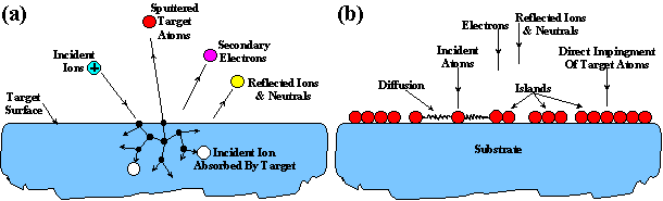
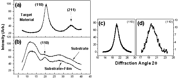
Figure 3.1: An illustrative diagram showing the sputtering process at the target (a), and film formation at the substrate (b).
| Growth and study of magnetostrictive FeSiBC thin films, for device applications, Mannan Ali (1999) | 32 | |
|---|---|---|
| (Online Copy) |
| Email:Mannan.Ali@physics.org | Chapter 3: General Experimental Techniques |
|---|---|
| Web: http://members.xoom.com/MannansZone/thesis.html |
of the substrate itself. Any surface defects or texturing of the substrates can effect the mobility of the incident atoms and will act as a barrier, and this can be reflected in the resulting properties of the film. The incident atoms with sufficient mobility will diffuse to join other incident atoms to form islands which will continue to grow until they coalesce to form a continuous film (see Wagendristel et al (1994) for details). Other species of particles besides the target atoms can also bombarded the substrate, which can influence the growth of the film. The neutral reflected atoms and gas particles are particularly difficult to control, as they cannot be manipulated using electric or magnetic fields. These particles can have sufficient energy on arrival at the substrate such that they sputter the film or become incorporated into the film itself. The bombardment of these particles can be controlled by working at pressures where the mean free path of the particles is small compared to the target-substrate separation, or by working at lower sputtering powers. In addition to these neutral particles, the substrate can also suffer bombardment from reflected gas ions. Control of these particles can be achieved by applying a bias to the substrate; this is known as bias sputtering. This effect has been extensively utilised in the study of magnetic films (Chapter 4). All particles impinging on the substrate, including electrons, will liberate energy in the form of heat, increasing the temperature of the substrate which effects the mobility of the target atoms and hence the depositing film.
3.1.2 Radio Frequency Magnetron Sputtering
In this study all magnetic films were grown by Radio Frequency (RF) magnetron sputtering using a Nordiko NM2000 system. The system is schematically shown in Figure 3.2. The sputtering system was configured to operate in the sputter-up mode, where the substrates were mounted 6cm directly above the target electrode. The sputter-up configuration had the advantage of not suffering from the problem of eroded target fragments falling on the substrate electrode and thus affecting the depositing film. Both the substrate and target electrodes were 15cm in diameter and were water-cooled. The Nordiko NM2000 consisted of three target electrodes (referred to as 1,2,3) which were mounted on a rotatable carousel. This provided the facility to sputter from three different target materials separately, and therefore allowed the deposition of multi-layered films. A grounded stainless steel shielding plate ensured that only the target below the substrate electrode was being sputtered from. In this study all films were grown using target electrode 1 unless otherwise stated. The importance of this is discussed in Section 5.8.1. The main chamber is attached to a mechanical hoist in order that the vacuum chamber could be lifted clear of the base of the machine to provide access for the mounting of targets and general maintenance. Two Viton seals were used to provide a vacuum seal for the main chamber as shown Figure 3.2. The rotatable shutters were positioned to provide shielding for either the target or substrate from the plasma. This allowed the target or substrate to be sputter-cleaned prior to the deposition of the film. A stainless steel clamping ring was used to secure the target to the copper electrode which ensured good electrical and thermal contact. To prevent sputtering from the clamping ring itself, an over-sized earthing shield was mounted directly above to prevent the plasma from coming into contact with the ring. The earthing shield also prevented the sputtered material from being deposited onto the insulator which isolated the target electrode from ground. Substrates were mounted
| Growth and study of magnetostrictive FeSiBC thin films, for device applications, Mannan Ali (1999) | 33 | |
|---|---|---|
| (Online Copy) |
| Email:Mannan.Ali@physics.org | Chapter 3: General Experimental Techniques |
|---|---|
| Web: http://members.xoom.com/MannansZone/thesis.html |

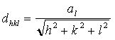
Figure 3.2: A schematic representation of the Nordiko NM2000 sputtering system used to sputter deposit the amorphous thin films.
on a removable copper substrate platter which interlocked firmly into the substrate electrode with a copper gasket which insured good thermal and electrical contact.
The power from the RF amplifier could be directed either to the target or the substrate electrode by means of a relay switch through a matching circuit. This allowed the impedance of the power supply and electrode to be matched, so the required power could be delivered efficiently. Directing the power to the substrate electrode allowed the substrates to be sputter etched if needed before the deposition of the film. The sputtering gas used was zero-grade high purity argon (99.99%); the gas flow was controlled by a needle valve and by partially opening the high vacuum baffle valve.
The high vacuum pumping system consisted of a diffusion pump (Balzers DIF 200) which was backed by a mechanical rotary pump (Balzers DUO 030A). A liquid nitrogen trap was situated between the high vacuum baffle valve and the diffusion pump so as to prevent oil or water vapour from entering the chamber. The chamber could be isolated from the pumping system by the high vacuum baffle value which allowed the chamber to be vented to atmospheric pressure without the requirement of shutting the pumping system down. The baffle valve also allowed the chamber to be gradually exposed to the high vacuum pumping system. This was important since the chamber was only evacuated to a pressure of 10-2 mTorr using the mechanical rotary pump, whereas the high vacuum pumping system was in the low 10-8 Torr region. Any sudden opening of the high vacuum valve would have resulted in oil vapour passing into the chamber, and disrupting the flow of the diffusion pump. Pneumatic valves were used to isolate or open the rotary pump to either the chamber or the diffusion pump. The chamber pressure was monitored by a Pirani gauge (A2) in the range 102-10-4 mTorr and by a cold cathode Penning gauge (B1)
| Growth and study of magnetostrictive FeSiBC thin films, for device applications, Mannan Ali (1999) | 34 | |
|---|---|---|
| (Online Copy) |
| Email:Mannan.Ali@physics.org | Chapter 3: General Experimental Techniques |
|---|---|
| Web: http://members.xoom.com/MannansZone/thesis.html |
in the range ~10-5-10-8 Torr. The foreline (backing) pressure for the diffusion pump was monitored using a second Pirani gauge (A1).
All removable items (earthing shields, shutters, etc.) within the chamber were shot-blasted using a fine glass bead prior to the growth of any FeSiBC films. This was to remove any foreign material which had previously been grown in the chamber. The sputtering process deposited material on all surfaces within the chamber, and therefore it could also sputter material back off these surfaces thereby contaminating the films (secondary sputtering). All items were de-greased after shot-blasting and handled with clean-room gloves. The chamber was periodically baked out at 700C to reduce out-gassing, and hence improve the vacuum. The contaminants within the system were monitored using a residual gas analyser (Balzers QMG64 RGA).
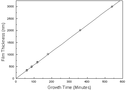
Use of a magnetron source increased the growth rate by ensuring that a high density of electrons exists near the surface of the target. The field from the magnetron forms a race track from where the majority of the material is sputtered. The downside to this is that the target erodes at a much higher rate in these regions, making very little use of the majority of the target. The growth rate is dependent mainly upon the pressure and power at which the films are deposited. The growth rate is also affected by substrate and target separation, but this was always fixed at 6cm. Increasing the sputtering power increases the growth rate and therefore erosion of the target, but it also has the effect of raising the temperature of the target and substrate. Increasing the pressure will also increase the sputtering rate at low pressures, but this will level off and even decrease at higher pressures because the various particles are slowed down by inelastic collisions. The magnetic properties of the films can be highly sensitive to pressure, power and the temperature at which they are deposited.
3.1.3 Target and Substrate preparation
The magnetic thin films studied throughout this thesis were sputter deposited from an amorphous METGLAS® 2605SC ribbon material of composition Fe81Si3.5B13.5C2. The material was supplied by the Allied Signal Corporation and came in the form of an amorphous melt-spun ribbon 18cm in width. The target used for sputtering consisted of two circular 15cm diameter targets which were carefully cut from the 18cm width melt-spun ribbon. The matt side of each target was lightly cleaned with iso-propanol/acetone and immediately dried in a stream of dry nitrogen gas. The two targets were then
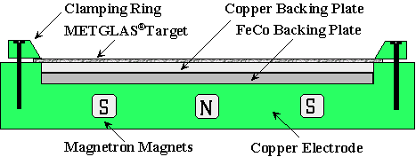
Figure 3.3: A diagram of the target electrode illustrating the mounting of the targets.
| Growth and study of magnetostrictive FeSiBC thin films, for device applications, Mannan Ali (1999) | 35 | |
|---|---|---|
| (Online Copy) |
| Email:Mannan.Ali@physics.org | Chapter 3: General Experimental Techniques |
|---|---|
| Web: http://members.xoom.com/MannansZone/thesis.html |
assembled on target electrode one unless otherwise stated, matt side up as shown in Figure 3.3. A 1mm thick copper and FeCo backing plate was also placed beneath the two METGLAS® 2605SC targets. The copper plate was used as a spacer and to protect the electrode and the FeCo disc from the plasma in the instances where the METGLAS® 2605SC targets eroded though. Two METGLAS® 2605SC targets were used to ensure that any small pinholes in the top target were covered by the target below, thus preventing any sputtering of the copper backing plate. The purpose of the FeCo plate was to increase the sputtering rate, since it increased the density of electrons near the target. The targets were clamped lightly to accommodate for thermal expansion and prevent shattering because of brittleness of the target after being heated during the sputtering process. The top target was changed after approximately 10 hours of growth at 75 watts or when the target shattered or eroded through.
The high quality of the deposited films was maintained by ensuring that the substrates were clean and grease free. This prevented the films from peeling away from the substrate and having imperfections such as pin holes. The glass-based substrates were ultrasonically de-greased, rinsed in acetone/isopropanol and dried in a stream of dry nitrogen gas. Silicon and GaAs substrates are extremely clean on purchase and were only cleaned by a stream of dry nitrogen gas to remove any surface dust particles. Kapton® substrates were cleaned in a similar manner to the glass-based substrates. Initially 1cm2 squared substrates were used. These were glued onto glass slides using a high temperature vacuum compatible glue. The substrates were always glued in the same positions for consistency. The glass slides were then clamped to the copper substrate holder as shown in Figure 3.4a. Further into the study, films were grown on substrates of dimensions up to 7.6cm by 2.6cm. In this case, substrates were mounted on the substrate holder using a picture frame design such that they were only held under their own weight. This eliminated any clamping forces upon the substrate. All substrates were handled with non-magnetic tweezers wherever possible, and using clean-room gloves. The acetone and isopropanol used in the preparation of the substrates were of the analar grade.
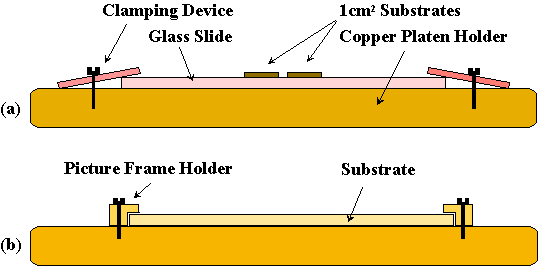
Figure 3.4: A diagram representing the two main types of holders used during the sputter deposition of the films in this study.
| Growth and study of magnetostrictive FeSiBC thin films, for device applications, Mannan Ali (1999) | 36 | |
|---|---|---|
| (Online Copy) |
| Email:Mannan.Ali@physics.org | Chapter 3: General Experimental Techniques |
|---|---|
| Web: http://members.xoom.com/MannansZone/thesis.html |
3.1.4 The deposition procedure
The growth of the films commenced once a low base pressure (B1) was established within the chamber in the low 10-7 Torr region. The high vacuum baffle valve was reduced to 30%, and a continuous flow of argon was allowed into the chamber via an inlet needle valve. The required pressure (A2) was obtained by careful adjustment of the needle valve which controlled the flow of argon into the chamber precisely. For consistency the baffle valve was always set to 30%, to ensure the same flow-rate of gas through the chamber during each growth. The continuous flow of argon into the chamber ensured that any gas contaminants produced by out-gassing of the chamber were removed. The plasma was ignited by setting the RF power to 20 W and then tuning the matching circuit so that the substrate or target impedance matched that of the power supply (50 Ohms). This was indicated by the reflected power; the smaller the reflected power, the better the match. The argon pressure was momentarily increased until the plasma has ignited using a second argon inlet valve. Once ignited the reflected power was readjusted to zero and the power was increased in steps of 1W to the required value.
During the initial stages of the study, the substrates were pre-sputtered to clean their surface prior to the deposition of the film. This procedure was later abandoned for reasons discussed in Chapter 4. The METGLAS® 2605SC ribbon targets were always pre-sputtered for the following reasons:
[1] It ensured that any contamination or oxidation of the surface of the ribbon targets which may have resulted during the fabrication process was removed, and therefore did not get incorporated into the depositing film.
[2] It allowed sufficient time for an equilibrium of sputtering particles to be established. At the start of sputtering, the target and surrounding chamber are cold and as the target heats up, the sputtering properties of the target will also change.
[3] Contamination of the films from secondary sputtering from the surrounding chamber environment is removed, since the chamber is coated with a thin layer of METGLAS® during the pre-sputter.
[4] It allowed an adequate length of time for any substantial out-gassing of the chamber and target to occur and an equilibrium state to be reached. This also allows the pumping system to reach an equilibrium state, which will ensure a constant flow of argon gas through the chamber and hence constant pressure.
[5] Finally it permitted the whole sputtering system to reach thermal equilibrium before the deposition of the film began.
There were two steps involved in the pre-sputter; the target was initially sputtered at 200 W for 15 minutes to remove any surface oxides and speed up any out-gassing processes (points [1] & [4]), the power was then reduced down to 75 W and sputtered for a further for 5 minutes to allow time for the target and surrounding environment to reach thermal equilibrium [points [2],[3] & [5]). At this stage the substrate shutter which is shielding the substrate from the plasma is rotated to commence the deposition of the film. The pre-sputter times were reduced to 10 and 5 minutes respectively for further growths of the same target. The time of 15 minutes at 200 W was only used for the first growth of each new target.
| Growth and study of magnetostrictive FeSiBC thin films, for device applications, Mannan Ali (1999) | 37 | |
|---|---|---|
| (Online Copy) |